ECE 5745 Final Project: Systolic Array based on Latency Insensitive Processing Element
Completed during the spring semester of my Masters of Engineering program.
While the introduction of various matrix extensions in architecture like Intel advanced Matrix extension, IBM PowerPC Matrix-Multiply Assist and Arm Scalable Matrix extension, it is clear that the architecture's development for supporting matrix operations is quite necessary. In this project we aim to design a matrix multiplication support unit which is coupled with a general purpose processor like a medium grained accelerator. This unit will receive commands from the processor when the processor writes to several Control/Status Registers (CSR’s). These commands will be decoded which tells this unit to load input operand matrix for a multiplication, carry out the multiplication and store the resultant matrix into the destination in the data cache and respond a done signal back to the processor. The matrix multiplication unit will be a systolic array which works on an output stationary algorithm. Each Processing Element(PE) will do a multiply accumulation to store the result in a memory element and will pass the two input operands to its adjacent processing elements. The functionality of a systolic array for matrix-matrix multiplication is explained in Figure1. In this 3x3 Matrix Multiplication example, there are 5 steps required to compute the resultant matrix C. In the first step, A[0][0] and B[0][0] enter the PE specific for C[0][0] and begin the multiplication process. The second step sees A[1][0] and B[1][0] entering the PE for C[1][0] as well as A[0][1] and B[0][1] entering the PE for C[0][1]. Following this pattern, if we assume that multiplication finishes within one cycle, the resulting matrix C would finish in 5 cycles. In software implementations created in C/C++, we would need a nested for loop to compute each PE serially, meaning that C[0][0] would execute, then C[0][1], and so on. This multiplication process would finish in 9 cycles under the same assumption stated before. As a result, we gain the benefit of reducing the number of overall cycles needed to finish the execution by 4 cycles.
As per our literature review this design technique would bring down the energy consumption of matrix multiply instruction at a performance benefit by reducing the number of memory operations and parallelizing matrix multiplication onto several PE’s. We prove this hypothesis in this project. We design an alternative design which is systolic array of various sizes which like 3x3, 4x4 and 10x10 to do respective matrix multiplication. The alternative design took only 20 cycles for completing a 3x3 multiplication while the baseline design takes close to 210 cycles. The alternative design is a standalone systolic array and is not capable of taking in instructions, hence not able to take care of loads and stores. It is tested with sources and sinks feeding the data. Hence the comparison of 210 and 20 is not apples to apples. However we were able to give the baseline processor a dummy C program which only loads two arrays of 9 elements each and stores an array of 9 elements to memory. This allowed us to compare the computation time of baseline as compared to our systolic. It is as close as we could compare a stand alone unit to a general purpose processor. The baseline design promises at least 8X performance improvement at a cost of additional 28523 um2, which is a good trade-off for any kind of accelerator. It consumes a 0.209 nj of energy for a 3x3 multiplication of positive numbers as compared to a baseline design which takes in 18 nj for the same task. (These comparisons have been made after subtracting the memory overload on the baseline so that it is a fair comparison).
The computational pattern in many graph algorithms involves transforming a set of active vertices to a new set of active vertices. Another application of graph algorithms is the workhorse of page rank algorithms used by Google to rank web pages. This algorithm computes a web page’s importance using matrix multiplication as the central kernel. One way to accelerate these algorithms would be to represent the graphs as matrices and take advantage of the duality between linear algebra and graph algorithms and compute the result using simple matrix multiplication. Applications in the machine learning domain have benefitted from high performing deep Convolutional Neural Networks (CNNs). Not surprising enough that the 90% of these neural networks computational expense is convolution. Scaling throughput of these convolution operations is limited due to the bandwidth and is energy expensive due to high amount of data movement. In such applications, the matrix sizes can be huge and we know that as matrix sizes grow, these computations can take significantly longer to execute, especially in a software implementation where we will see an execution time growth of O(N2), where N is the size of the input matrices. Hence, we recognized that matrix multiplication is the need in today's applications and all domains using the above discussed algorithms would benefit multifold from specialized matrix units/accelerators.
One of the supporting examples of above inference is, a custom ASIC i.e. Tensor Processing Units (TPUs). It has been used since 2015 in data centers which have proven to improve the inference phase of Neural Networks (NN) . The TPUs have been optimized to perform at several TeraOps/second by improving the design of basic MAC (multiplication accumulate unit) using systolic execution [1]. Rather than adding a matrix multiply unit inside a CPU, we decided to explore a more TPU like unit using a systolic array made up of multiply-accumulate units coupled with a processor through internal commands which can be fed to this unit through CSR’s like an accelerator. The major motivation behind this design decision was that the control unit for such units takes far less hardware on the die as compared to adding support in a CPU/GPU [1] which allows us to have the bandwidth of using larger systolic array sizes and load buffers improving performance while using dedicated area for useful work. As we know that for matrix-matrix multiplication, one of the major bottlenecks is the communication with memory which is much more energy expensive than arithmetic operations. A simple matrix multiplication unit would have to wait for memory to respond with the complete input matrices. Even if we parallelize the computation, two 10X10 matrices having 32 bit integer values need to be multiplied it could take (N2) * (N2) operand loads and takes N2 resultant stores on a memory bus width of 32 bits. This is a lot of cycles and is a lot of work, hence increases energy expense. The motivation behind using systolic array units is to save energy by reducing reads and writes of the matrix unit [2][3][4]. The systolic array depends on data from different directions arriving at relevant Processing Elements (PE) in an array at regular intervals where they are combined.
As discussed earlier CNNs have provided huge performance benefits in machine learning algorithms varying from image recognition, facial recognition, object detection to navigation and genomics. In order to improve the performance of CNN’s parallelising data flow and data processing has proven to be beneficial. The main idea behind these designs is that the dataflow unit is responsible for mapping data to memory banks in a way that maximizes data reuse, while the processing unit performs computations on the data in a highly parallel manner. [6] One such example is the Eyeriss spatial architecture. It has been proven that such architectures, when run on several benchmark CNNs and compared to other state-of-the-art spatial architectures, achieve significant energy savings while maintaining high performance, especially for CNNs with large filter sizes. With the increasing trend of integrating machine learning in smaller devices, for example cellular devices and embedded systems, it is a necessity to bring down the power consumption
The article "Energy-Efficient Hardware Accelerators for Machine Learning" presents a series of hardware accelerators, collectively referred to as the DianNao family, specifically designed for Machine Learning (ML) applications, with a particular focus on neural networks. The authors emphasize the importance of addressing memory transfer efficiency in the design of these accelerators to maximize performance and energy savings. This literature review will explore the concept of loop tiling in the DianNao family, and how this can be used to design a systolic array in hardware for a given project. The author's motivation stems from the growing prevalence of ML tasks in various applications and the increasing reliance on neural network-based techniques like deep learning as a unique opportunity for designing accelerators with broad application scope, high performance, and efficiency. Current ML workloads are mostly executed on multi-cores using SIMD, GPUs, or FPGAs, which may not fully exploit the potential of hardware accelerators. The authors argue that inefficient memory transfers can negate the benefits of accelerators, and therefore should be a first-order concern in their design.
The DianNao family comprises four hardware accelerators: DianNao, DaDianNao, ShiDianNao, and PuDianNao. The accelerators are designed specifically for ML applications, with an emphasis on neural networks. They focus on minimizing memory transfers and maximizing memory usage efficiency. A key concept in the DianNao family is the utilization of loop tiling to minimize memory accesses and efficiently accommodate large neural networks. Loop tiling involves splitting the computation into smaller blocks, reducing the memory bandwidth requirements of each layer. The authors demonstrate a ~50% reduction in memory bandwidth requirements for a classifier layer using this technique. The idea of loop tiling can be extended to design a systolic array in hardware for a given project. Systolic arrays are a type of parallel computing architecture that can efficiently perform matrix operations, which are common in ML applications. In a systolic array, data flows through an array of processing elements (PEs), each performing a partial computation and passing the result to the next PE. By applying loop tiling in the design of a systolic array, the memory access overhead can be reduced, and the overall performance and energy efficiency of the hardware can be improved. The loop tiling technique can be used to partition the computations performed by the systolic array into smaller blocks, allowing the PEs to work on subsets of the data in parallel. This approach reduces memory bandwidth requirements and helps to balance the workload among the PEs.
We attended one of the deep dives in Batten's Research Group (BRG) where one of the Phd Students - Tuan Ta was talking about their work on adding support for sparse matrices in general purpose CPUs. The talk motivated us to explore the idea of implementing a systolic array in hardware and pushing it through the ASIC flow and do a performance, power and area analysis on how it works with dense multiplication when used as a coarse grained accelerator. We thank him for leading us towards this idea. We would like to acknowledge professor Christopher Battens contribution in allowing us to think in a more deeper way which led us to the idea of designing a matrix unit loosely coupled with the processor which works on certain internal commands from the processor to accelerate the dense matrix-matrix multiplication. We would also like to acknowledge Christopher Battens contribution to our deep level understanding of ASIC flow and RTL designing through ECE 5745 and ECE 4750 coursework. Also, we would like to acknowledge professor Zhiru Zhang for helping us understand the basics of systolic arrays through ECE 5775 coursework. We would also like to acknowledge one of our fellow student Aidan's contributions who went ahead and created a datapath diagram for the 5 stage pipeline processor with the accelerator interface support.
The baseline design for the project is a pure-software matrix-matrix multiplication microbenchmark running on a pipelined processor with its own instruction and data cache from ECE 4750 lab 4. The matrix_multiplication() function in ubmark_matrix_mult.c, has 6 parameters. It takes an input matrix A, an input matrix B and returns an output matrix C. The input “n” for number of rows for matrix A, input “m” for number of columns for matrix A and “p” for number of rows dimension for matrix B. As with any matrix multiplication, the rows in A and columns in B need to be the same i.e. input “m” to produce an “n” X “p” sized output matrix C. Before discussing the algorithm, we need to clarify how the input matrices A and B and output matrices are stored in memory. For our design, we dynamically allocate memory in the form of an array, sizing the memory appropriately to cover the total number of indices in the matrix and multiplying the total number by (int)sizeof(int), when calling ece4750_malloc. By only creating an array in memory instead of an actual matrix, we can manipulate how the values in the array are stored to appropriately act as a matrix. The image I have created below illustrates how basic matrix multiplication works and how we implemented our array based calculation.
Since we are not directly indexing parts of a matrix as shown in the Matrix Multiplication section, we needed to ensure we are correctly indexing parts of the A and B arrays. The algorithm above shows how we do that indexing and provides an example of that calculation. Additionally, the colors underneath each calculation are used to show which index those calculations refer to. Following the algorithm we described, we performed our matrix multiplication using three nested for loops. The first for loop ranges from an integer “i” to the row dimension “n” of matrix A. The next for loop iterates from an integer j to the column dimension “p” of matrix B. Lastly, the innermost for loop iterates from an integer k to “m”, the column dimension of matrix A and the row dimension of matrix B.
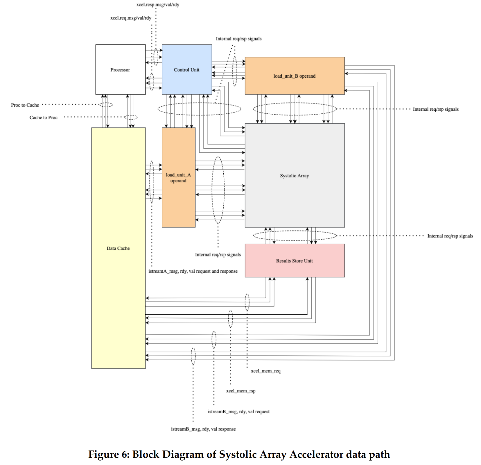
Figure 1 illustrates the overall system we will be using in this project which integrates a processor, accelerator and instruction and data cache memories.. The processor includes eight latency insensitive val/rdy interfaces. The mngr2proc/proc2mngr interfaces are Design for Test (DFT) interfaces which are used to send data to the processor and for the processor to send data back to the test harness. The imemreq/imemresp interfaces are used for instruction fetch, and the dmemreq/dmemresp interfaces are used for implementing load/store instructions. The system includes both instruction and data caches similar to lab4 in ECE 4750.. The xcelreq/xcelresp interfaces are used for the processor to send messages to the accelerator. In order to keep the baseline design without any accelerator we use a null accelerator similar to Lab 2 in ECE 5745. This unit can be ignored as all the workload of matrix multiplication is carried by the processor alone and the null is just a placeholder for the accelerator unit while pushing through the ASIC flow.
The processor we use is a five-stage pipelined processor that implements the TinyRV2 instruction set and includes full bypassing to resolve data hazards which is from Lab2 in ECE4750. Unlike Lab2 the processor design uses a single-cycle integer multiplier. We verified in Lab2 ECE 5745 that when the design is pushed through the flow the single-cycle integer multiplier does not adversely impact the overall processor cycle time. Second, the new processor design includes the ability to handle new Control/Status Registers (CSRs)for interacting with medium-grain accelerators. We will be leveraging these CSRs which are 32 in number in order to create special commands from processor to accelerator/matrix multiply unit, for example “load matrix” in special matrix load unit, “go” command to run the systolic array multiplier, “store matrix” into the memory through a special matrix store unit.
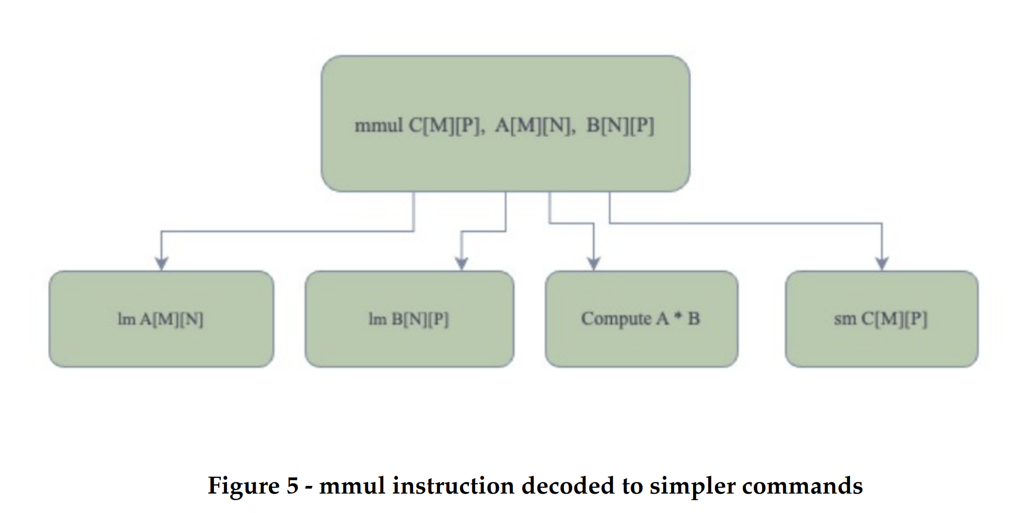
To implement a matrix multiplication unit we decided to design a matrix-multiply unit, which is decoupled from the processor, similar to an accelerator approach in ECE 5745 Lab2. We chose to add a loosely coupled unit which functions as a co-processor, similar to a TPU design. This design decision was made because it would allow us to have a less complex processor control logic and separate control for the matrix-multiply unit. Adding this support within the CPU/GPU control logic have proven to take a higher area on the die[1] as compared to keeping it loosely coupled with the processor.. Our alternative design consists of the same processor as discussed in the previous section, which is now connected with a matrix-multiply unit.The xcel master/minion interface is used for the processor to send messages to the matrix-multiply unit.. The processor can directly send/receive messages to/from the unit with special instructions. The matrix-multiply unit is designed to consist of a control unit, two load operand units, a store result unit and a systolic array. The matrix-multiply unit will include a set of accelerator registers that can be read and written from the processor using special instructions through xcelreq/xcelresp interface. The processor will send messages to the accelerator by reading and writing 32 special CSRs using the standard CSRW and CSRR instructions. These 32 special CSRs. One of the first step in designing the alternative design was to understand how a matrix multiply operation would carry out in a general purpose processor. While doing this we found that the complex matrix multiplication instruction could be divided into simpler commands (similar to micro-ops). We then designed an RTL module for carrying out each command. This illustrates the incremental design approach and the modularity principle as each command's functionality is represented by a module in our design. As shown in figure 5 a matrix multiplication instruction “mmul” could be interpreted as two “lm” type commands, meaning to load matrix A and B. A command to compute the multiplication result and a command “sm”, meaning store matrix into the address of C. The load unit A and B are responsible for carrying out the first two commands. The systolic array is designed to carry out the third command and the store matrix unit is designed to carry out the last command. The design and functionality of each unit is discussed in detail in the subsequent subsections.
The control unit is designed to read a go signal from the processor. This means when the control unit sees a write in the xr0 register, it interprets it as a “go” signal for the matrix unit. Once this signal is received, the control unit moves to the LOAD_OPERANDS state. This state activates the load operand unit A and B. Once the load units completely fetch the input operands from the data memory, they send out a done signal to the control unit. The control unit, now moves to the COMPUTE state which activates the systolic array by sending a “compute” signal. Once the systolic array has completely accumulated the result, it sends out a done signal to the control unit. The control unit FSM moves to the COLLECT_RESULT state. This state sends out a give_result signal to the systolic array and the store result unit. Now the systolic array starts to push the result to the store result unit. Once the result is completely pushed out, the systolic sends out a “fed” result to the control unit. The control unit, now moves to the WRITE_RESULT state. In this state, a “write” signal is sent out to the write result unit, which writes the result to the data cache. Once the store unit completes writing the data memory with the resultant matrix C[i][j], it sends a “done” bit to the control unit. This “done” bit moves the control unit to DONE state. In this state the control unit reads the xr0 for done.
The load operand units communicate to the control unit through latency insensitive master/minion interface and istream message, valid, and ready latency insensitive interface for communicating with the systolic array. These units also have a 96 bit xcelmem master/minion communication interface to read three 32 bit values at once in the memory. We know that this is a big memory port but we decided to have wider memory ports in order to keep the implementation simple and focus on performance benefits due to the systolics. We might change the port width to a more realistic one, once the systolic implementation is towards completion.
The load operand units A and B receive a start signal from the control unit. Once it is received, the load operand A unit reads the xr1 and xr2 to read the base address of the matrix A and the size of matrix A respectively. Similarly, the load operand B unit reads the xr3 and xr4 to read the base address of the matrix B and the size of matrix B respectively. This information sets a signal to start fetching the data from the data cache in the respective load units through the xcelmem master/minion interfaces. The xcelmem response sets a done_fetch signal which is sent back to the control unit to mark the completion of operand collection. (Tentative design)
This is the central unit of our alternative design. Once, the module receives a “compute” signal from the control unit, it starts receiving inputs from the load units A and B through the 6 latency insensitive interfaces. As discussed earlier, we decided to implement the systolic array to compute the resultant matrix as per the output stationary algorithm. To implement this, the west input interface receives the input values of matrix A in a row-major order, from load operand unit A. The north input stream receives the input values of matrix B in a column-major order, from load operand unit B. The systolic array is a 9 time instantiation of a single processing element (PE) in a 3x3 fashion in which one input matrix data flows from West-to-east direction and the other matrix data flows from North-to-South direction while multiplying and accumulating the result when the corresponding operands meet in the respective PE. This functionality is shown in Figure 7. The PE design logic is discussed in detail in the subsequent subsection. In order to understand systolics better, we have named the signals as per the direction in which the data flows in a systolic array.
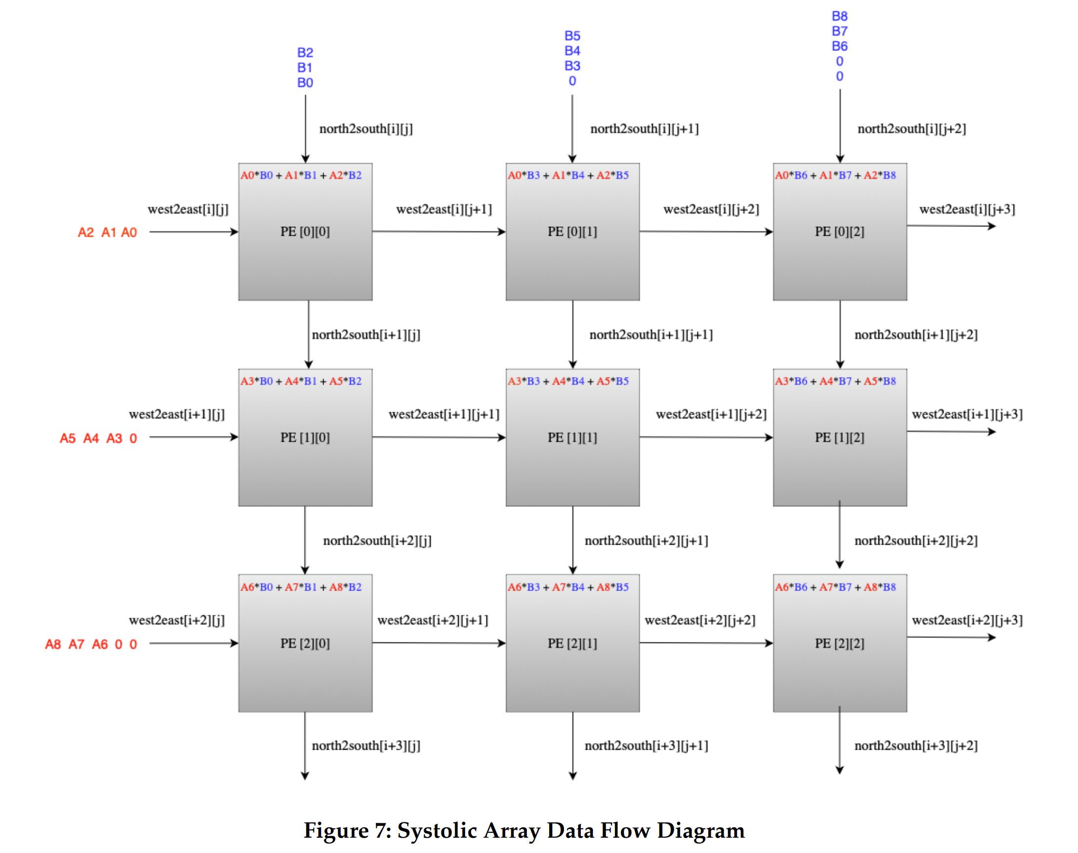
As you can see, the input data from input matrix A through istreamA0-A3 flows in West-to-East direction using wires West-toEast[i][j] and the the data from input matrix B through istreamB0-B3 flows in North-to-south direction using wires North-to-South[i][j]. Each processing element PE[i][j] takes in inputs from the West and North, multiplies and accumulates the result. This PE[i][j] sends out the western inputs to PE[i][j+1] through the eastern output interface and sends out the northern inputs to the southern output interface to PE[i+1][j]. This communication between PE’s allows us to compute the correct matrix multiply result. For a 3x3 matrix multiply, the systolic will have each element of the resultant matrix C[i][j] stored in the corresponding PE[i][j] at the end of 7 cycles. At this point the control unit will send a “feed_result” signal to the systolic array. This feed_result will flush out the accumulated results from each PE in 3 cycles through the wires flowing north to south. These results are communicated to the store unit through the ostream interface of the systolic array which is also a master/minion interface.
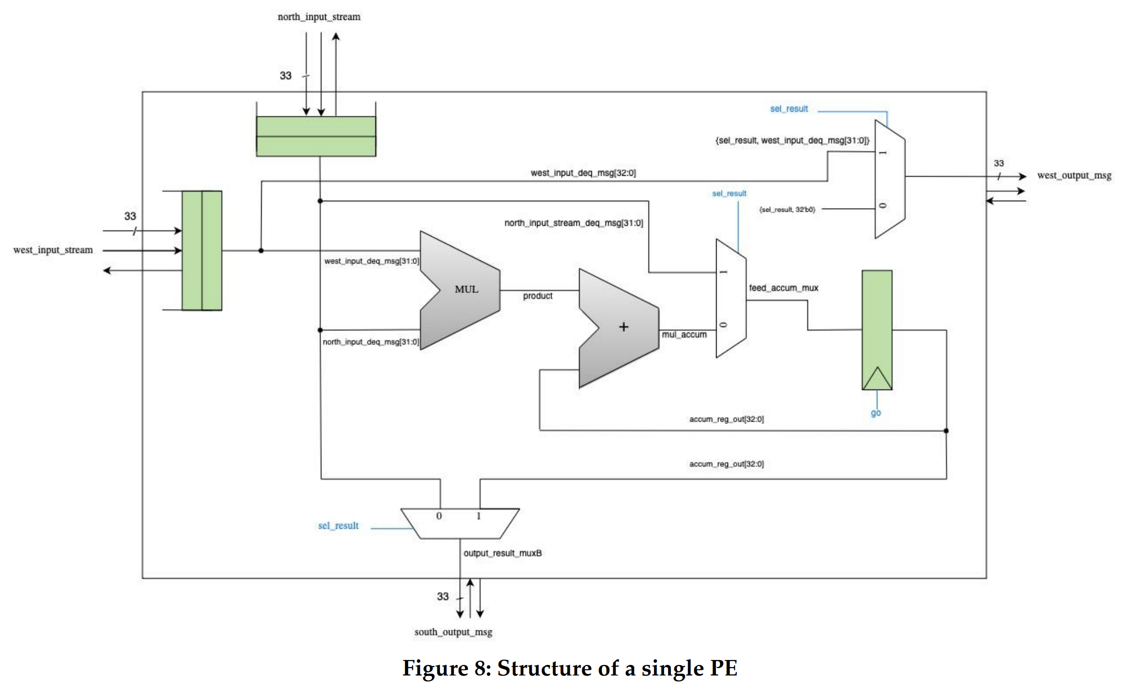
In order to implement the systolic array we needed to design a single processing element first. The processing element for a systolic array needed to have a multiplication accumulation functionality and the ability to store the inputs and pass it to the next PE in the next cycle. In order to achieve this, our PE design has 4 latency insensitive interfaces. The west input stream interface receives a 33 bit input from the west. The north input stream interface receives a 33 bit number from the North. These input messages and val signals are enqueued in the input queues . The deq messages are fed to a multiplier and the multiplication output is accumulated in an accumulator. The west output interface sends out the value from either the deq message of the west input or a zero, depending on the sel_result bit towards the east direction and the south output interface sends out the value from deq or the accumulated register towards the south direction. If the first bits of both input messages are 1, then the PE enters int give result mode which means it sends out the accumulated result out the south direction and zeros in the east direction. These bits becoming 1 are controlled by the control logic which are concatenated with the memory messages and fed to this PE. In the current implementation our test sources send these bits in the input messages depending on the mode we want to enable.
A possible design for this unit would be that the store unit communicates to the control unit through xmem valid and ready latency insensitive master/minion interface and ostream message, valid, and ready latency insensitive interface for communicating with the systolic array. The store unit also has a 96 bit xcelmem master/minion communication interface to write three 32 bit values at once in the memory. We know that this is a big memory port but we decided to have wider memory ports in order to keep the implementation simple and focus on performance benefits due to the systolics. We might change the port width, once the systolic implementation is towards completion.
The store result unit receives a “collect_result” signal from the control unit. Once it is received, it sets the systolic-store unit interface rdy as high and starts storing data into a 9 element buffer. Once it receives the data, the control unit has also received a “fed” signal from the systolic. In the WRITE_RESULT state, the unit reads the xr5 to read the base address of the resultant matrix C. This information sets a valid signal on the xcelmem request signal which allows the unit to start writing the stored 9 elements into the data memory. Once this step is complete, the store result unit sets the “done” signal using the last memory write response. This “done” signal moves the control unit to the DONE state.
Keeping it decoupled from the processor, the design approach would allow us to have a separate unit which works on simple commands that can be decoded and pass request type signals to different modules within the unit. We aim to follow the principle of encapsulation and modularity in our design. Each unit in the design will be a separate module and the implementation details would be hidden from the neighbors.
In order to get the baseline working functionally we used the simplest adhoc testing initially where the matrix_multiply() function was passed with constant size matrix inputs, for example we fed the function with a 3X3 matrix as operand A and a 3X3 matrix as operand B while expecting a resultant C matrix of size 3X3. We were entirely depending on printing the inputs A, B and resultant C in order to verify the functionality. However, like hardware testing, ad-hoc testing is not sufficient as it is not an automated process and requires a lot of user interaction in observing the outputs which are printed. This would not allow us to have a robust testing methodology. Hence, we designed a C -testing framework for our baseline software design similar to the one in ECE5745 Lab2. We wrote multiple tests in a single test.c file and ran all those on our matrix multiplication program. Firstly, this test.c file was built and tested natively. Natively compiling and executing means that we test our program by compiling it on ecelinux for x86 assembly and then execute this program on the ecelinux server itself using a C test bench. This step was important to catch bugs in our C program for matrix multiplication early because trying to debug an error in a C program while running it on a processor simulator or RTL model could get painful and difficult to narrow down.
To test our C software natively we call a configure script in the app/ build-native which uses the makefile in the app folder as a template to create a specialized makefile for this folder. Once it is built for the X86 assembly we can execute the binary file on ecelinux. The table 1 describes multiple directed tests we implemented for testing the program. While directed test cases covered a good part of the program, we still needed random testing. This is because random testing improves the coverage and gives a chance to test the unexplored corner cases of an algorithm which direct testing alone would not be able to accomplish. We used the ece4750_rand() function in order to generate random numbers from the ece4750 standard C library. Again, we could not use the standard C library as those would not cross compile on our processor RTL model as it does not have an Operating System, hence the standard randint() functions were out of scope.
When we call the c-test file it uses five files that would aide in our testing and evaluation - ubmark-matrix-mult.c, ubmark-matrix-mult.h, ubmark-matrix-mult.dat, ubmark-matrix-mult-test.c, ubmark-matrix-mult-eval.c. We implemented the matrix multiplication in ubmark-matrix-mult.c. This file only includes the matrix_multiplication() function. Inside our test harness we instantiate both matrices A and B by allocating space on the heap and assigning each matrix specific values (whether by passing constant values and dimensions, or randomly testing by passing these as a parameter). We also allocate space on the heap for our result and reference matrix, C and C_ref, and through the use of a for loop, preemptively set every index to be 0. These matrices, A, B, and C are then passed into our matrix_multiplication() function and the result matrix C is returned. In order to test if our matrix multiplication is working correctly, we wrote a golden reference which creates a C_ref by passing the same inputs A and B to a matrix_multiply_reference(). We now compare the output matrix C to our C_ref through the use of the function compare_matrices(). This function compares the values of each index in the arrays and ensures they are the same. If they are not, the test fails.
As we have learnt in ECE 4750 and ECE5745, this is the advantage of writing a robust test harness where we just need to pass values through input parameters and the harness will take care of feeding it to the Design Under Test (DUT), feeding it to a golden reference model and then collecting results in a module and comparing these. The user only gets a prompt whether the test passed or failed. This is similar to any hardware testing. Moreover, it also has a flavor of UVM methodology where our compare_matrices() is analogous to UVM’s monitor module and the matrix_multiply_reference() is analogous to UVM’s golden reference module. The generate_random() function is analogous to the driver module in UVM while the DUT is our matrix_multiply() function. UVM is used for hardware testing but we extrapolated the same idea in our software testing too.
The hardware testing strategy is yet to be discussed as that would be our alternative design testing. However, we have started implementing a simple Multiplication accumulate unit which takes in two 32 bit numbers and gives a 32 bit result while passing the input operands as it is. (We plan to instantiate this unit in an NXN systolic array which uses the output stationary method). We have tested it exhaustively using the pymtl3 testing framework similar to ECE 5745 labs. So far we have tested the multiplication accumulate unit with the test cases discussed in the table below. In here as well, we have had a combination of directed and random testing. These test cases will also help for our whitebox testing of the systolic array as it tests the internal functionality of a given RTL unit.
| Test Case | Type | Description |
|---|---|---|
| test_case_1_mult_A11_B11 | Directed | Test case for small size matrix operands A[1x1]*B[1x1]=C[1x1] |
| test_case_2_mult_A11_B11_zero | Directed | Test case for small size matrix operands A[1x1]*B[1x1]=C[1x1] with zero values |
| test_case_3_mult_A22_B22 | Directed | Test case for small size matrix operands A[2x2]*B[2x2]=C[2x2] |
| test_case_4_mult_A22_B22_zero | Directed | Test case for small size matrix operands A[2x2]*B[2x2]=C[2x2] with zero values |
| test_case_5_mult_A33_B33 | Directed | Test case for small size matrix operands A[3x3]*B[3x3]=C[3x3] |
| test_case_6_mult_A33_B33_zero | Directed | Test case for small size matrix operands A[3x3]*B[3x3]=C[3x3] with zero values |
| test_case_7_mult_A44_B44 | Directed | Test case for small size matrix operands A[4x4]*B[4x4]=C[4x4] |
| test_case_8_mult_A44_B44_zero | Directed | Test case for small size matrix operands A[4x4]*B[4x4]=C[4x4] with zero values |
| test_case_9_mult_A55_B55 | Directed | Test case for small size matrix operands A[5x5]*B[5x5]=C[5x5] |
| test_case_10_mult_A55_B55_zero | Directed | Test case for small size matrix operands A[5x5]*B[5x5]=C[5x5] with zero values |
| test_case_11_mult_A23_B32 | Directed | Test case for small size matrix operands A[2x3]*B[3x2]=C[2x2] |
| test_case_12_mult_A23_B32_zero | Directed | Test case for small size matrix operands A[2x3]*B[3x2]=C[2x2] with zero values |
| test_case_13_mult_A33_B32 | Directed | Test case for small size matrix operands A[3x3]*B[3x2]=C[3x2] |
| test_case_14_mult_A33_B32_zero | Directed | Test case for small size matrix operands A[3x3]*B[3x2]=C[3x2] with zero values |
| test_case_15_mult_A43_B35 | Directed | Test case for small size matrix operands A[4x3]*B[3x5]=C[4x5] |
| test_case_16_mult_A43_B35_zero | Directed | Test case for small size matrix operands A[4x3]*B[3x5]=C[4x5] with zero values |
| test_case_17_mult_A43_B31 | Directed | Test case for small size matrix operands A[4x3]*B[3x1]=C[4x1] |
| test_case_18_mult_A43_B31_zeros | Directed | Test case for small size matrix operands A[4x3]*B[3x1]=C[4x1] with zero values |
| test_case_19_mult_A51_B15 | Directed | Test case for small size matrix operands A[5x1]*B[1x5]=C[5x5] |
| test_case_20_mult_A51_B15_zero | Directed | Test case for small size matrix operands A[5x1]*B[1x5]=C[5x5] with zero values |
| test_case_21_mult_A53_B31 | Directed | Test case for small size matrix operands A[5x3]*B[3x1]=C[5x1] |
| test_case_22_mult_A53_B31_zero | Directed | Test case for small size matrix operands A[5x3]*B[3x1]=C[5x1] with zero values |
| test_case_23_mult_basic | Random | Test case for small size matrices, A[3x3]*B[3x3]=C[3x3] with random values between 0 and 5 |
| test_case_24_mult_five_element | Random | Test case for small size matrices, A[5x5]*B[5x5]=C[5x5] with random values between 0 and 5 |
| test_case_25_mult_small_zeros | Random | Test case for small size matrices, A[3x5]*B[5x3]=C[3x3] with random values between 0 and 5 |
| test_case_26_mult_one_element | Random | Test case for small size matrices, A[1x1]*B[1x1]=C[1x1] with random values between 0 and 5 |
| test_case_27_mult_two_elements | Random | Test case for small size matrices, A[2x2]*B[2x2]=C[2x2] with random values between 0 and 5 |
| test_case_28_mult_larger_matrix | Random | Test case for larger size matrices, A[10x10]*B[10x10]=C[10x10] with random values between 0 and 5 |
| test_case_29_mult_larger_matrix_larger_values | Random | Test case for much larger size matrices, A[25x25]*B[25x25]=C[25x25] with random values between 0 and 100 |
| test_case_30_mult_max_size_small_values | Random | Test case for max size matrices, A[32x32]*B[32x32]=C[32x32] with random values between 0 and 5 |
| test_case_31_mult_max_size_medium_values | Random | Test case for max size matrices, A[32x32]*B[32x32]=C[32x32] with random values between 0 and 100 |
| test_case_32_mult_max_size_large_values | Random | Test case for max size matrices, A[32x32]*B[32x32]=C[32x32] with random values between 0 and 1000 |
| test_case_33_mult_max_size_very_large_values | Random | Test case for max size matrices, A[32x32]*B[32x32]=C[32x32] with random values between 0 and 10,000 |
| test_case_34_mult_max_size_even_larger_values | Random | Test case for max size matrices, A[32x32]*B[32x32]=C[32x32] with random values between 0 and 100,000,000 |
Our alternative design consists of multiple latency insensitive design units. We developed these units incrementally and kept on unit testing before integrating the next unit in order to catch any bugs at an earlier stage, hence following an incremental and modular design approach. In this project we have used the pytest unit testing framework from ECE4750. The pytest framework is popular in the Python programming community with many features that make it well-suited for test-driven hardware development including: no-boilerplate testing with the standard assert statement; automatic test discovery; helpful traceback and failing assertion reporting; standard output capture; sophisticated parameterized testing; test marking for skipping certain tests; distributed testing; and many third-party plugins. In order to use pytest we kept all our tests in a subdirectory “test” inside the “systolic” subdirectory
Our test harness composes stream source(s), a latency-insensitive Design Under Test (DUT) , and a stream sink(s). When constructing the test harness we pass in a list of input messages for the stream source to send to the DUT and a list of expected output messages for the stream sink to check against the messages received from the DUT. The stream source and sink take care of correctly handling the val/rdy micro-protocol. All our directed and random test cases use the above methods to confirm the functionality of each unit.
However, it is not enough to just test the functionality of the design, it is also important to make sure that a unit functions correctly even if the neighboring units are delayed due to stalls. When a module uses a latency insensitive interface, it might receive two kinds of events. First kind of event are informative events, which means that in this case the signals would be carrying valid data and actual work needs to be done. The other type of event is <>. This means that the DUT should treat the received data in this tenure as invalid as the unit next to it is stalling
It was important to test that each individual unit module works correctly in a combination of both types of events. In other words, we want to make sure that the design under test sends the exact same output when handling arbitrary source/sink delays as compared to when not under delay. The stream source and sink components enable setting an initial_delay and an interval_delay to help with this kind of delay testing
We created a test case table in python and used pytest.mark.parametrize to pass the respective columns of the test case table to source, DUT and sink units. For example in Table 2
| Test Case Table | msgs | srcA delay | srcB delay | sinkA delay | sinkB delay |
|---|---|---|---|---|---|
| small_pos_pos_3in | small_pos_pos_3in_msgs | 0 | 0 | 0 | 0 |
| small_pos_zero_3in | small_pos_zero_3in_msgs | 0 | 0 | 0 | 0 |
| large_pos_pos_3in | large_pos_pos_3in_msgs | 0 | 0 | 0 | 0 |
| large_pos_zero_3in | large_pos_zero_3in_msgs | 0 | 0 | 0 | 0 |
When testing our Systolic Array, we needed to directly test the inputs and outputs of each PE, meaning we needed source and sink delays for every PE. Figure 10 below only shows source and sink delays for A0, A1, B0, and B1 to save space, however when testing more complex designs, we needed to include the delays for all inputs and outputs. Just like with the test case table for a single PE, each of these tests included 10 more tests with different delays, though they are not shown to save space. Hence we were able to test our design with all combinations of delays which increased the test coverage and made a total test cases as 360 in addition to the integration testing which is shown in Table 3.
| Test Case Table | msgs | srcA0 delay | srcB0 delay | srcA1 delay | srcB1 delay | sinkA0 delay | sinkB0 delay | sinkA1 delay | sinkB1 delay |
|---|---|---|---|---|---|---|---|---|---|
| small pos pos 3x3 1 | small pos pos 3in msgs | 0 | 0 | 0 | 0 | 0 | 0 | 0 | 0 |
| small pos pos 3x3 2 | small pos zero 3in msgs | 0 | 0 | 0 | 0 | 0 | 0 | 0 | 0 |
| small pos pos 3x3 3 | large pos pos 3in msgs | 0 | 0 | 0 | 0 | 0 | 0 | 0 | 0 |
The first unit to test was our basic processing element. Based on the functionality of this unit we tested this unit with different types of input data types ranging from small positive positive numbers to large negative negative numbers to make sure that the sign bit does not fail our design functionality. We also used various sequences of zeros and pure zero messages in order to make sure that zeros are treated correctly. In addition to these directed test cases, we also feed the processing element with random inputs on both the streams and make sure that we receive the expected output. This type of test case was important to increase the testing coverage of the design.
As discussed, the delay testing for each unit was important. Since our PE would be instantiated 9 times in the systolic array and this systolic array is supposed to be integrated with 4 more units, it was even more important to delay testing the PE’s before moving forward. Since the PE has 4 latency insensitive interfaces, we tested with four different sources and sinks and varying all the possible combinations of delays.
This delay testing helped us to recognize a bug. Our North to South dataflow and West to East dataflow was originally independent of each other. In a systolic array, this meant that if a PE[i+1][j] is stalling not ready to receive an input for some reason, while the PE[i][j+1] is ready, the matrix A data would flow in West to East direction, and the matrix B data would not be able to flow from North to South. Hence, computing a wrong matrix multiplication result. This bug would have been really tedious to debug if this issue was recognized in the integration state. Since we were testing a single PE at this point, it was easy to recognize that when we gave varying sink delays at southern and eastern output ports, the PE fails to give the expected result. A quick fix to this was making the input streams ready only if both the eastern and southern output streams receive a ready signal. This shows the importance of unit testing and the advantages of a modular approach. TableN shows all the tests which we wrote for a single PE.
Once the native C testing was complete we could cross compile the matrix-multiplication algorithm for RISC-V assembly using “riscv32-unknown-elf-gcc” which is the cross-compiler for RISC-V. We build and execute this section in a separate directory to keep the native C testing and the cross compilation testing at different locations. This executable was then tested on an RTL model of the RISC-V based fully bypassed 5 stage pipelined processor. The results of these runs will be discussed more in the Evaluation section (TBD). In order to evaluate the baseline design we wrote a function that generates random matrices in the form of an array (however, we kept the seed of the ece4750_rand a constant in order to keep the tests reproducible). By using this function, we populated a ubmark-matrix-mult.dat file that's integral to the project's evaluation phase. This function generated two input matrices of 10X10 dimension which were fed to the software multiplication algorithm running on the processor. When we put the stats on for this command we got a total number of cycles over 10,000 which is 10 times the cycles taken by the processor for running the ubmark_vvadd program for input matrices of 100 elements. This was the expected result as the matrix-multiplication is a triple nested loop which would definitely have more number of instructions in the RISC-V assembly code which was confirmed by seeing the resultant assembly code for both programs. We saw an increase in the number of instructions by a factor of 11x when we compared the ubmark evaluation results for matrix multiplication and vvadd shown in Figures 5 and 6. However, we would aim to bring the number of cycles down with our alternative design while trading off between the increase in area and the increase in performance between the two.
For evaluating our baseline design, we ran multiple instances with varying input matrix sizes, ranging from 2x2 to 20x20, using only even numbers at this point. Our evaluation code uses two preset matrices stored in a .dat file and performs the matrix multiplication on those two matrices. As we increased the size of the input matrices, we noticed that regardless of the size of the values in each matrix when the size is kept constant, the total number of cycles and instructions did not change. However, this is a direct result of the single cycle multiplier that's used in the processor. Each multiplication requires two loads and a store instruction, which helps explain why the instructions also do not change with increasing values. However, when we increased the dimensions of the input matrices, from a 2 by 2 to a 4 by 4, as an example, we see a significant increase in the total number of cycles and instructions required. Table 4 below stores the number of cycles, instructions, and the CPI for every iteration and the energy usage for a select few designs we pushed through the flow. (TBD: more will be computed if we feel necessary). One thing that is important to note is that for every iteration of the Baseline design, the total area of the design did not change. This is due to the fact that the baseline design is purely the processor, with no additional hardware being created.
| Baseline Design Input Matrix Size | Number of Cycles | Number of Instructions | CPI | Energy | Power |
|---|---|---|---|---|---|
| 2x2 | 158 | 141 | 1.12 | ||
| 3x3 | 397 | 342 | 1.16 | 21.4624 nJ | 3.519 mW |
| 4x4 | 832 | 703 | 1.18 | 31.6651 nJ | 3.455 mW |
| 6x6 | 2530 | 2097 | 1.21 | ||
| 8x8 | 5732 | 4707 | 1.22 | ||
| 10x10 | 10918 | 8917 | 1.22 | 280.239 nJ | 3.755 mW |
| Alternative Design Input Matrix Size | Number of Cycles | Number of Instructions | CPI | Energy | Power |
| 3x3 | 20 | 0.2094 nJ | 1.047 mW | ||
| 5x5 | 28 | 3.84 nJ | 6.659 mW | ||
| 10x10 | 48 | 7.68 nJ | 16 mW | ||
| Dummy Unit: Load and Store | Number of Cycles | Number of Instructions | CPI | Energy | Power |
| 3x3 | 99 | 82 | 1.21 |
To keep the evaluation denominator constant, we wanted to focus on the performance of a 3x3 systolic array against the 3x3 multiplication on the baseline design. While the baseline design took 397 cycles to complete a 3x3 matrix multiplication, the alternative design took only 20 cycles to do the same. We are aware that the baseline design runs an entire assembly code of the matrix matrix multiplication which includes 18 loads and 9 stores from the memory in addition to the matrix multiplication. And an overhead of branching in order to run the for loop(s). However we tried to closely evaluate the two implementations. In order to do that we ran a dummy code on the baseline design which only did 18 loads and 9 stores. This was a simple C code which loads 9 elements from 2 sources each and stores only 9 elements out of those to a destination memory location, without any computation overhead. When we subtracted this cycle count from the original baseline cycle count for matrix multiplication, we got a total number of cycles to be 321. The comparison of this number and our systolic implementation cycle count is much more realistic. We are aware that this comparison might still not account for a few other instructions but it still shows that 321 cycles against 20 cycles is a huge improvement. Even if we consider a load unit and a store unit integrated with the systolic, it will still be orders of magnitude better than the baseline general purpose multiplication.
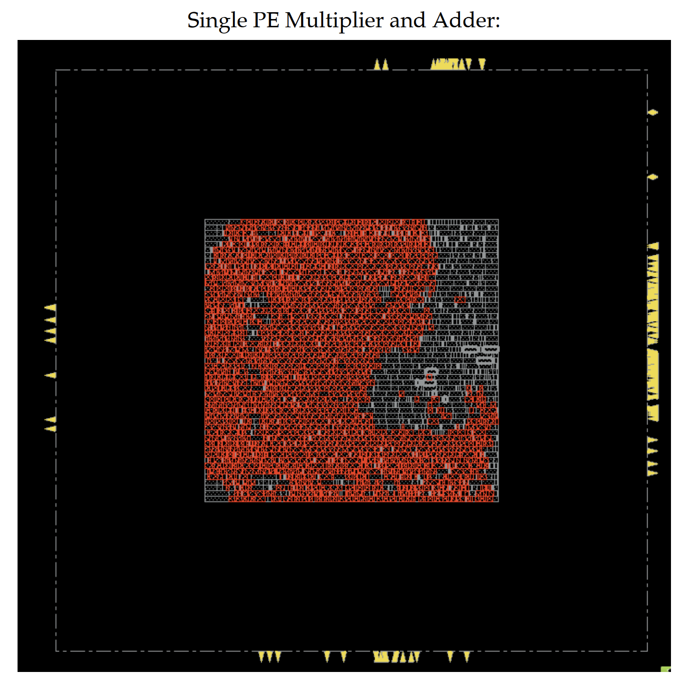
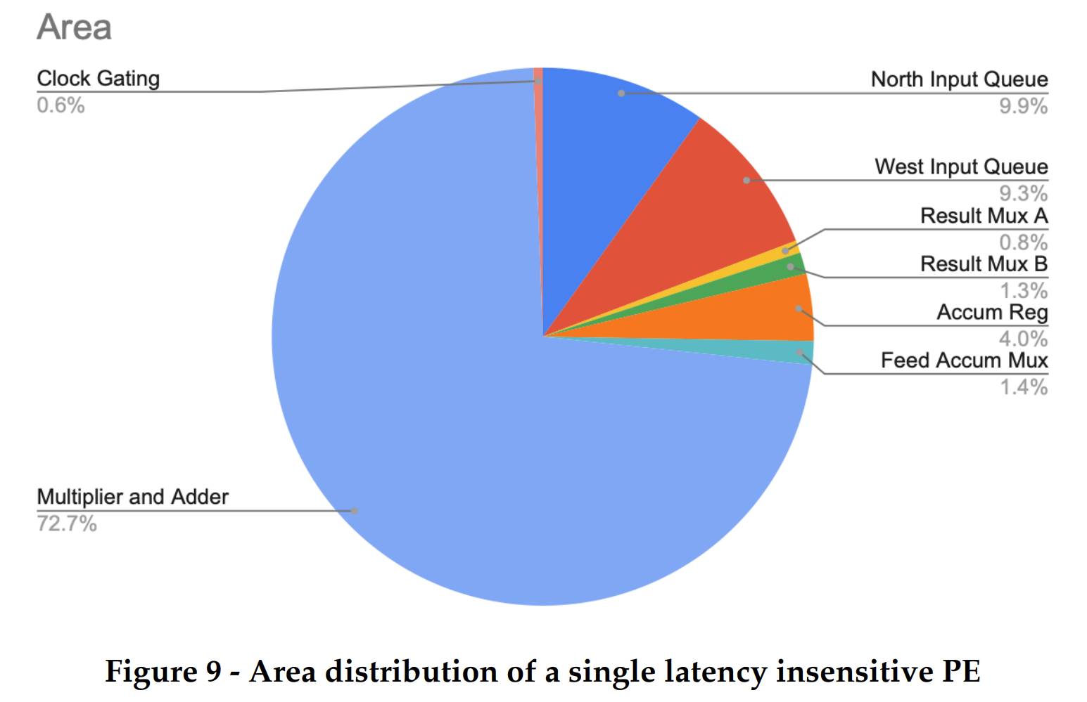
As we pushed our baseline design, alternative design and the individual PE through the flow we got a lot of insights about the area usage. For a single PE, the total design area was 4643.5 um2. Almost 73 percent of this area is taken up by the module DP_OP_5J1_123_5558 which implements the combinational logic of multiply accumulation. This was expected as the multiplication accumulation is the center of our matrix multiplication to store the partial products. Our design choice of adding 2 element 33 bit normal queues came at a cost. These queues occupy a total of 20% area of the design. However this is a good tradeoff as this queue would allow our PE to send requests for the new row/column of the matrix from the memory while the PE has still not finished the previous multiplication accumulation. Hence it decouples the functionality of the systolic from the time taken by the memory to respond. This is where our PE behaves as a latency insensitive module.
The additional normal queue also reduces the combinational delay of propagating back the rdy signal at the cost of added area due to registers that reduce the critical path of the logic. This was important to ensure that we do not make memory accesses, the critical path of our systolic unit. The muxes used to feed the outputs and the accumulator register do not take more than 1% area. The accumulator register does take 4% area of the design. However, this is also central to the multiplication accumulation functionality, hence it was a non-negotiable price to pay. We were able to notice the clock gating takes 0.6% area on the chip. It is interesting to note that the 2 queue registers and the accumulator registers were clock gated with the enable signal of these registers. This is a very small price to pay for switching off the power consumption of our sequential logic when it is not needed. This would bring down the total dynamic power consumption of the design and also reduce activity on the clock tree and activity on local intra-cell clocking logic.
Once we understood the area distribution of each PE, it was easy for us to analyze the area of our different systolic implementations. Our systolic array consists of NxN processing elements where N is the number of rows of matrix A/ columns in Matrix B. When we see Table 2, we can clearly see that the total area of the array is NxN times the area of a single PE. Since our implementation of each PE is latency insensitive, there was no need for additional control logic to get all the PE’s to work together. This saved us area as compared to a probable latency sensitive PE. We can see that the systolic array of 10x10 takes a whopping 317010.55 um2. However, it is understandable as it has 100 multipliers, 100 adders and 200 input queues. In future, we could add a control logic to this systolic array which would allow us to tile a given size matrix as per the size of the systolic and each tile can be computed in a smaller systolic size for a 10x10 multiplication. This would add an overhead for control logic and a performance dip by increasing the number of total cycles, but it would certainly save a lot of area by reducing the number of multiply-accumulate units required to do the same amount of work.
| Systolic Size | Number of PE's | Design Area (um2) |
|---|---|---|
| 3X3 | 9 | 28523.446 |
| 5X5 | 25 | 79238.74 |
| 10X10 | 100 | 317010.554 |
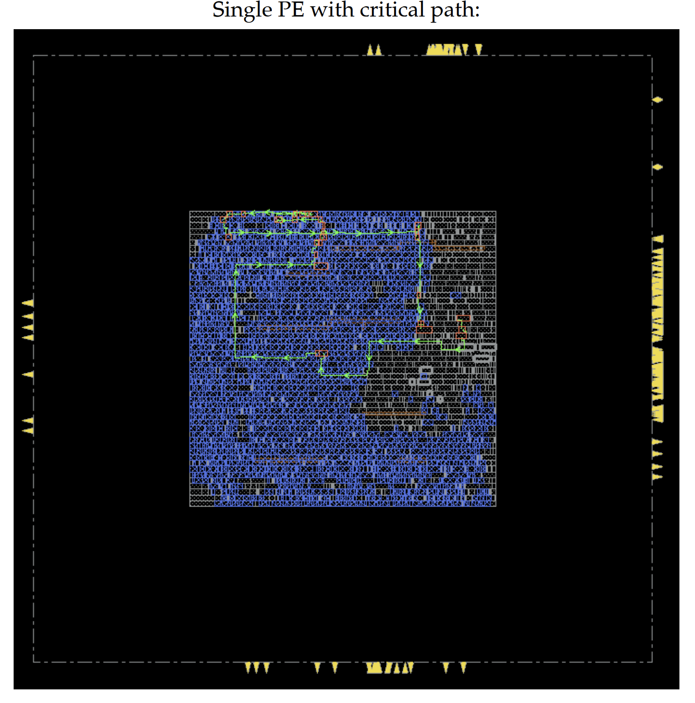
As a result of the post synthesis timing report, we were able to analyze the timing of each PE and our various systolic designs. Like the area, we analyzed the timing of a single PE first. The clock frequency of a single PE came out to be 3.6 ns which was higher than the constraint of 3 ns which we have used for the accelerator design so far in our design.Although our PE exceeds the constrained clock but since our implementation is more focused for a GPU/TPU like implementation unit. These units focus more on throughput than the latency. For such design units, if we are able to do enough work in parallel, then we can pay the cost of higher latency. Our design allows that by having input normal queues which would be increasing the throughput by keeping fetching and storing subsequent row/columns while the systolic is computing the result. Hence, like a pipelined processor, this unit will also keep giving a result in each cycle after the entire systolic has been filled with the data. That being said, we still wanted to analyze the critical path of our PE. As we can see in figure 10, the critical path starts from a register inside the west_input_queue, goes through multiplier, adder, then to the feed accumulator mux and ends at the accumulator register. As intended the critical path starts from a register inside the unit, hence when we integrate memory with our design, the memory access would not be the critical path. The latency of the PE would always depend on the combinational delay of only the multiplication accumulation step. We can see in the figure that the critical path highlighted in green traverses majorly in the multiplier-adder (blue). This means that if we were able to pick a better standard cell design for this functionality with a lesser propagation delay, we could have met the 3.0 ns timing constraint as well. In the future scope, we would also like to experiment with different adder and single cycle multiplication implementations in order to see the impact on timing.
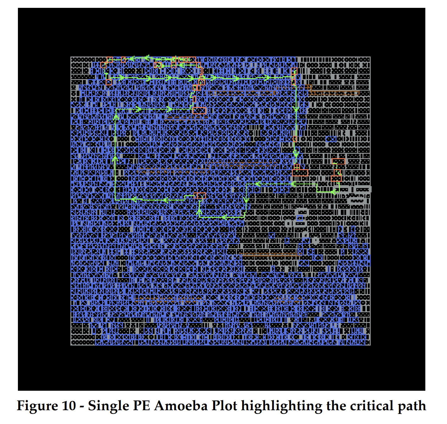
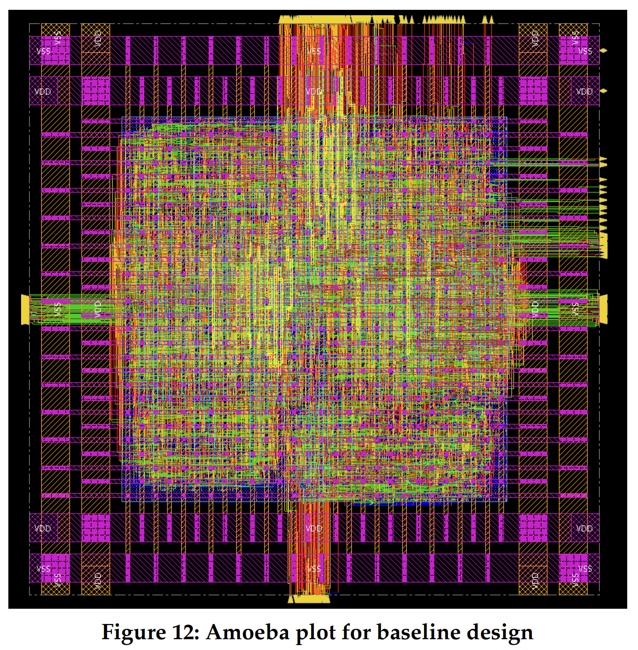
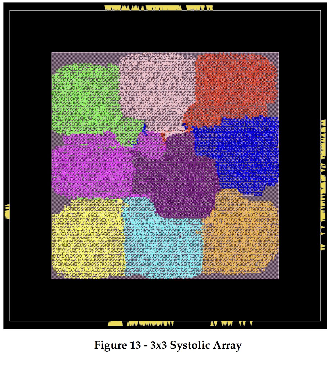
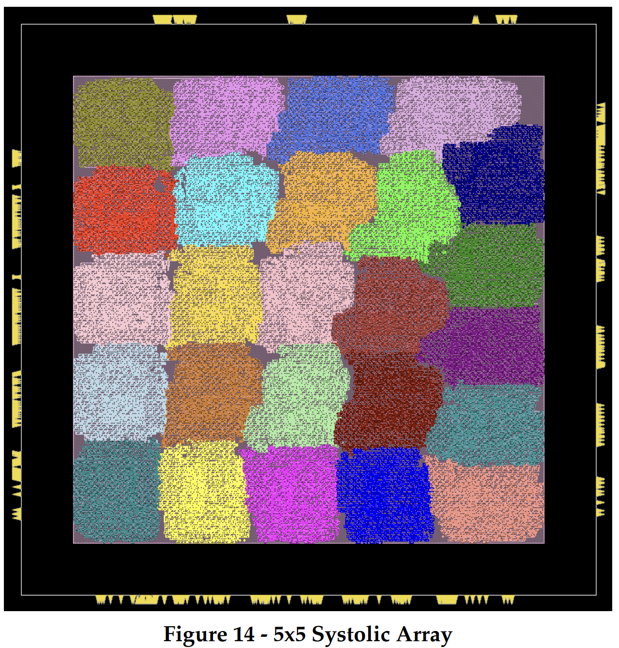
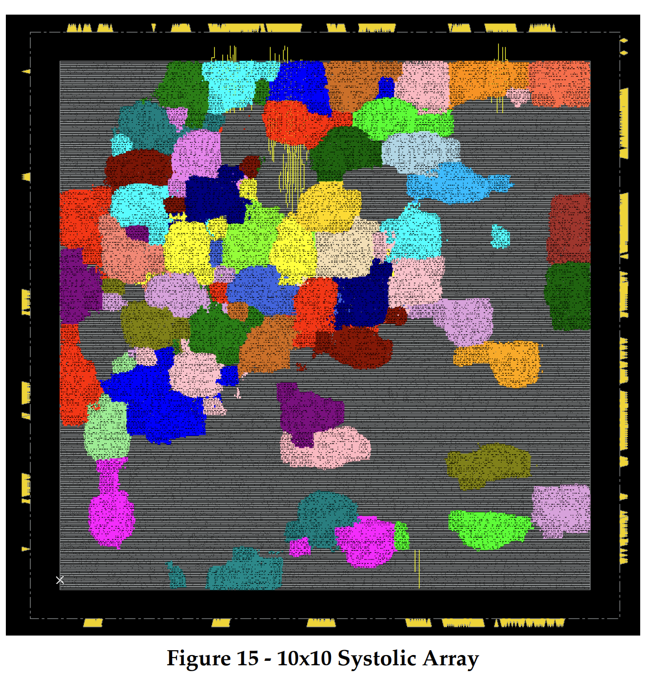
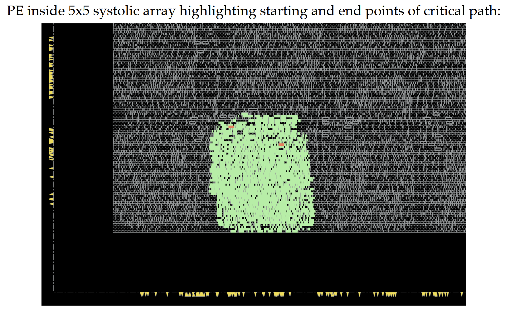
Now that we know the critical path for our single PE we were able to evaluate the timing reports of our 3x3, 5x5 and 10x0 systolic arrays. As you can see in figure 11, the amoeba plots of all systolic implementations have different PE’s highlighted. In each implementation the critical path lies in one of the PE’s with the same route traversing from an input queue to the single cycle multiplier, adder, feed accumulator mux and ends at the accumulator register. One other advantage of using the Normal queues can be noticed here. In case we chose to implement without the queues, the entire design would have had a long combinational path for the rdy signal traversing from the input of the systolic array to all the PE’s and increasing the cycle time. Since, the rdy path has been cut by multiple queues in the entire design, the cycle time for the design remains the same as a single PE.
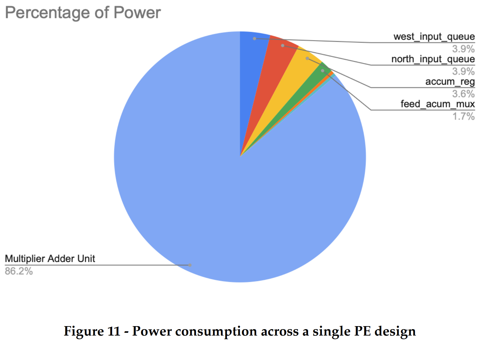
We also observed the power consumption of our design. As expected, the most power consumed was by the multiplier and adder which constituted 86% of the total dynamic power consumed. The power consumed by the sequential logic parts like the queues, accumulator reg were 3.9% and 3.6% respectively. These numbers could have been higher if the tool did not enable clock gating. Since the enable signals for these registers were clocked with their input clock, it reduced the activity on the clock tree and activity on local intra-cell clocking logic, hence bringing down total dynamic power consumption. This can clearly be seen in figure 11.
One of the supporting examples our inferences that matrix multiplication units benefit machine learning is - Tensor Processing Units (TPUs). It has been used since 2015 in data centers which have proven to improve the inference phase of Neural Networks (NN) . The TPUs have been optimized to perform at several TeraOps/second by improving the design of basic MAC (multiplication accumulate unit) using systolic execution [1]. Rather than adding a matrix multiply unit inside a CPU, we decided to explore a more TPU like unit using a systolic array made up of multiply-accumulate units coupled with a processor through internal commands which can be fed to this unit through CSR’s like an accelerator. The major motivation behind this design decision was that the control unit for such units takes far less hardware on the die as compared to adding support in a CPU/GPU [1] which allows us to have the bandwidth of using larger systolic array sizes and load buffers improving performance while using dedicated area for useful work.As we know that for matrix-matrix multiplication, one of the major bottlenecks is the communication with memory which is much more energy expensive than arithmetic operations. A simple matrix multiplication unit would have to wait for memory to respond with the complete input matrices. Even if we parallelize the computation, two 10X10 matrices having 32 bit integer values need to be multiplied it could take (N2) * (N2) operand loads and takes N2 resultant stores on a memory bus width of 32 bits. This is a lot of cycles and is a lot of work, hence increases energy expense. The motivation behind using systolic array units is to save energy by reducing reads and writes of the matrix unit [2][3][4]. The systolic array depends on data from different directions arriving at relevant Processing Elements (PE) in an array at regular intervals where they are combined.
The concept of loop tiling can be adapted to develop a systolic array in hardware for a specific project. Systolic arrays, a form of parallel computing architecture, can effectively execute matrix operations commonly found in ML applications. In such an array, data moves through a series of processing elements (PEs), with each performing a portion of the computation and forwarding the result to the next PE. Incorporating loop tiling into the systolic array's design can minimize memory access overhead and enhance the overall performance and energy efficiency of the hardware. Loop tiling can be employed to divide the computations carried out by the systolic array into smaller sections, enabling PEs to process data subsets simultaneously. This method lowers memory bandwidth needs and helps distribute the workload evenly among the PEs.
CNNs have provided huge performance benefits in machine learning algorithms varying from image recognition, facial recognition, object detection to navigation and genomics. In order to improve the performance of CNN’s parallelising data flow and data processing has proven to be beneficial. The main idea behind these designs is that the dataflow unit is responsible for mapping data to memory banks in a way that maximizes data reuse, while the processing unit performs computations on the data in a highly parallel manner. [6] One such example is the Eyeriss spatial architecture. It has been proven that such architectures, when run on several benchmark CNNs and compared to other state-of-the-art spatial architectures, achieve significant energy savings while maintaining high performance, especially for CNNs with large filter sizes. With the increasing trend of integrating machine learning in smaller devices, for example cellular devices and embedded systems, it is a necessity to bring down the power consumption.